1. NeuroSim
NeuroSim is a circuit-level macro model for benchmarking neuro-inspired architectures based on CMOS or emerging memories, which could estimate the circuit-level performance metrics, such as chip area, latency, dynamic energy and leakage power. NeuroSim could be integrated with neural network algorithms to become an integrated framework with hierarchical organization from the device level (transistor and analog synaptic device properties) to the circuit level (array architectures with periphery circuit modules) and then to the algorithm level (neural network topology), enabling trace-based and cycle-accurate evaluation on the accuracy as well as the circuit-level performance metrics at the run-time of learning or inference.

There are three versions of NeuroSim:
- MLP+NeuroSim: The target users are device engineers who wish to quickly estimate the system-level performance with his/her own synaptic device data including SRAM, RRAM, PCM, STT-MRAM and FeFET with digital row-by-row read-out or analog parallel read-out. As a case study, multilayer perceptron (MLP) and MNIST dataset are used. The integrated MLP+NeuroSim framework is developed in C++ and run in Linux system. The latest released version is V3.0 DOWNLOAD
- DNN+NeuroSim: The target users are circuit/architecture designers who wish to quickly estimate the system-level performance with near-memory or in-memory computing architectures. This is an integration of our NeuroSim circuit macro model with Tensorflow/PyTorch within Python environment. User could run hardware-compatible quantized training for accuracy and generate the circuit-level performance inference engine with various device technologies for large-scale dataset (CIFAR and ImageNet) using convolutional neural network topologies (VGG and ResNet). The latest released version for inference is V1.4 DOWNLOAD and for training is V2.1 DOWNLOAD
- 3D NeuroSim: This is an extension on top of the DNN+NeuroSim V 1.3 to enable electrical-thermal co-simulation of 3D integrated CIM accelerators. Two types of 3D integration are supported: one is monolithic 3D with back-end-of-line (BEOL) transistors and the other one is heterogeneous 3D with through-silicon-via (TSV) and hybrid bonding. The latest released version for inference is V1.0. DOWNLOAD
Copyright of the model is maintained by the developers, and the model is distributed under the terms of the Creative Commons Attribution-NonCommercial 4.0 International Public License http://creativecommons.org/licenses/by-nc/4.0/legalcode. If you use this model in your work, you are requested to cite [1] [2] or [3] in the reference.
Developers and contact information:
Ming-Yen Lee, James Read, Junmo Lee, Anni Lu, Xiaochen Peng, Shanshi Huang, Yandong Luo, Pai-Yu Chen, and Shimeng Yu
For technical questions, address to Ming-Yen Lee
For logistic questions, address to Prof. Shimeng Yu
References:
[1] P.-Y. Chen, X. Peng, S. Yu, “NeuroSim+: An integrated device-to-algorithm framework for benchmarking synaptic devices and array architectures,” IEEE International Electron Devices Meeting (IEDM) 2017, San Francisco, USA.
[2] P.-Y. Chen, X. Peng, S. Yu, “NeuroSim: A circuit-level macro model for benchmarking neuro-inspired architectures in online learning,” IEEE Trans. CAD, vol. 37, no. 12, pp. 3067-3080, 2018.
[3] X. Peng, S. Huang, Y. Luo, X. Sun, S. Yu, “DNN+NeuroSim: An end-to-end benchmarking framework for compute-in-memory accelerators with versatile device technologies,” IEEE International Electron Devices Meeting (IEDM) 2019, San Francisco, USA.
2. RRAM Verilog-A model for SPICE simulation
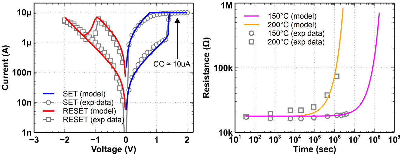
The Verilog-A compact model is developed for metal-oxide based RRAM devices with bipolar switching characteristics [1]. It is improved based on the earlier work originally developed at Stanford [2]. The parameters of the model are re-fitted to the experimental data of IMEC HfOx-based RRAM devices [3-4]. This Verilog-A model is compatible with common SPICE simulators, although HSPICE H-2013.03-SP2 is the recommended software. To demonstrate the model, an HSPICE netlist for 1T1R configuration is provided as an example.

Copyright of the model is maintained by the developers, and the model is distributed under the terms of the Creative Commons Attribution-NonCommercial 4.0 International Public License http://creativecommons.org/licenses/by-nc/4.0/legalcode. If you use this model in your work, you are requested to cite [1] in the reference.
Developers and contact information:
Pai-Yu Chen, and Shimeng Yu
For technical/logistic questions, address to Prof. Shimeng Yu
DOWNLOAD
References:
[1] P.-Y. Chen, S. Yu, “Compact modeling of RRAM devices and its applications in 1T1R and 1S1R array design,” IEEE Trans. Electron Devices, vol. 62, no. 12, pp. 4022-4028, 2015.
[2] X. Guan, S. Yu, and H.-S. P. Wong, “A SPICE compact model of metal oxide resistive switching memory with variations,” IEEE Electron Device Letters, vol. 33, no. 10, pp. 1405-1407, 2012.
[3] Y. Y. Chen, B. Govoreanu, L. Goux, R. Degraeve, A. Fantini, G. S. Kar, D. J. Wouters, G. Groeseneken, J. A. Kittl, M. Jurczak, and L. Altimime, “Balancing SET/RESET pulse for endurance in 1T1R bipolar RRAM,” IEEE Transactions on Electron Devices,vol. 59, pp. 3243-3249, 2012.
[4] Y. Y. Chen, M. Komura, R. Degraeve, B. Govoreanu, L. Goux, A. Fantini, N. Raghavan, S. Clima, L. Zhang, A. Belmonte, A. Redolfi, G. S. Kar, G. Groeseneken, J. A. Kittl and M. Jurczak, “Improvement of data retention in HfO2/Hf 1T1R RRAM cell under low operating current,” IEEE International Electron Devices Meeting (IEDM), pp. 252-255, 2013.
3. Emerging Memory Trend (2016)
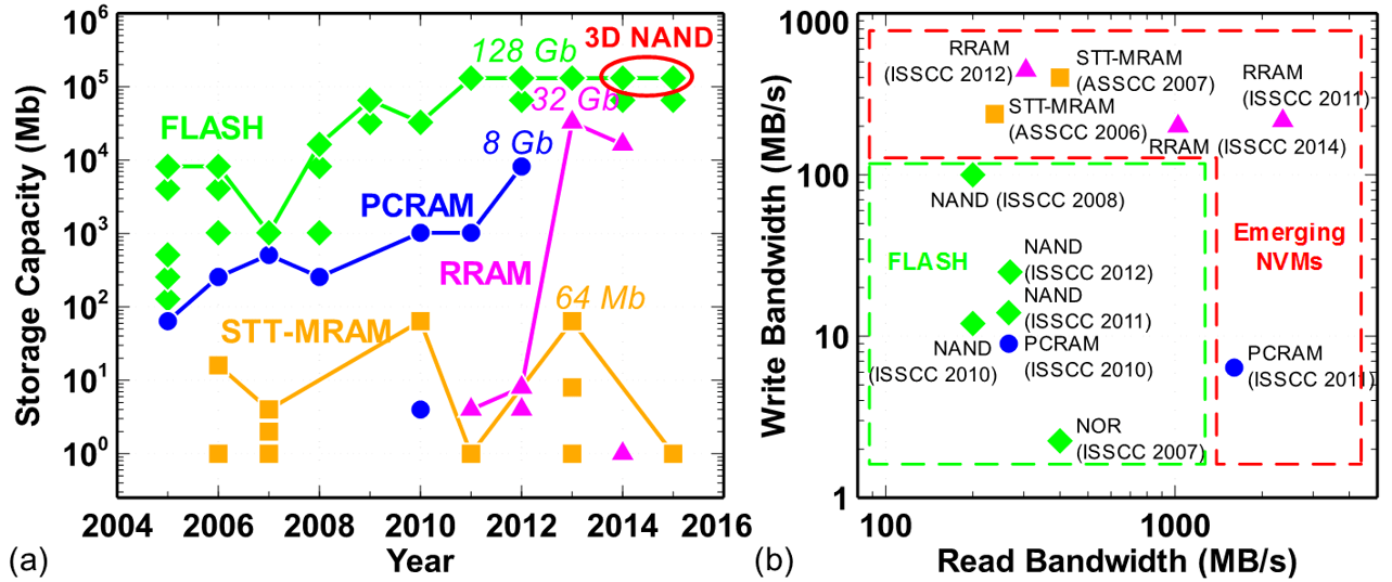
Emerging memory trend summarizes the recent prototype chip demonstrations of various emerging NVM technologies reported in the major conferences (e.g. IEDM, VLSI, ISSCC, etc.) from 2005 to 2015. It includes the memory capacity vs. year, and the write/read bandwidth versus year. The PCRAM and RRAM have demonstrated >Gb-level capacity owing to the smaller cell size (4 F2 using cross-point array or 6 F2 using 1T1R array with minimum sized transistor), while STT-MRAM’s capacity is only up to 64 Mb level (cell size is still >30 F2 owing to a larger transistor used to deliver sufficient write current in the 1T1R array and a relaxed layout design rule). It is noted that the bandwidth is related to the I/O interface. NAND FLASH typically use page-program (e.g. 4 kb per page) to achieve high bandwidth, although it has slow write time per cell. Emerging NVM macros typically do not use wide-I/O (only 64 or 128-bit interface) but has fast write-time-per-cell. Despite the narrow I/O, the emerging NVMs remarkably improve the write/read bandwidth over the NAND or NOR FLASH.

This datasheet also shows the silicon CMOS low-power logic transistor’s drive current with the scaling from 130 nm down to 20 nm for different W/L simulated with the Predictive Technology Model (PTM). Representative write current of STT-MRAM, PCRAM, RRAM from the literature data are also marked. RRAM’s write current typically ranges from 10 µA to 100 µA (with some scattered data points for sub-10 µA), and it does not scale with the device area due to the filamentary conduction mechanism. Although STT-MRAM and PCRAM’s write current scale with the device area, at 20 nm node, STT-MRAM’s current is ~40 µA, and PCRAM’s current is ~100 µA. It is seen that in most cases, W/L=1 transistors could not provide sufficient write current for NVM cell, thus 6 F2 cell area is unlikely to achieve using logic-compatible process. Although the transistor’s gate voltage (Vgs) can be boosted under the specially engineered DRAM process to increase the drive current, however it is still limited. For example, the drive current at Vgs=5 V can approach 40 µA for a W/L=1 transistor at 27 nm node [2]. Therefore, reducing the write current down to sub-10 µA by device engineering is of great importance for continuing the scaling of the 1T1R array.
The data sheet of the prototype chip parameters (e.g. capacity, performance, etc.) can be accessed via the following link.
Copyright of the figure and the datasheet are maintained by the developers, and they are distributed under the terms of the Creative Commons Attribution-NonCommercial 4.0 International Public License http://creativecommons.org/licenses/by-nc/4.0/legalcode. If you use the figure and/or the datasheet in your work, you are requested to cite [1] in the reference.
Developers and contact information:
Pai-Yu Chen, and Shimeng Yu
For technical/logistic questions, address to Prof. Shimeng Yu
References:
[1] S. Yu, P.-Y. Chen, “Emerging memory technologies: recent trends and prospects,” IEEE Solid State Circuits Magazine, vol. 8, no. 2, pp. 43-56, 2016.
[2] J. Zahurak, K. Miyata, M. Fischer, M. Balakrishnan, S. Chhajed, D. Wells, H. Li, A. Torsi, et al., “Process Integration of a 27nm, 16Gb Cu ReRAM,” IEEE International Electron Devices Meeting (IEDM), 2014.
