Overview:
Projects:
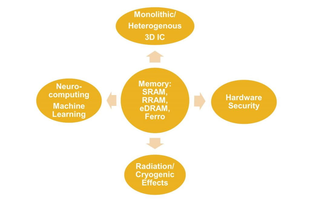
I. Emerging Non-Volatile Memories (eNVMs)
eNVMs include the spin-transfer torque magnetic random-access memory (STT-MRAM), phase change memory (PCM), resistive random access memory (RRAM) and ferroelectric field-effect transistor (FeFET). These eNVMs are mostly pursued as the next-generation storage-class memory or embedded memory technologies with aggressive industrial research and development, and we have extensive research activities in HfO2 based RRAM and ferroelectric devices. We are interested in the following topics:
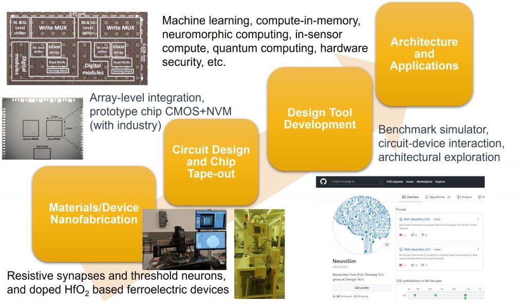
1. Nanofabrication: new material stack/device structure optimization through the atomic-layer-deposition (ALD); back-end-of-line (BEOL) process integration on top of CMOS coupon wafer.
2. Device testing and modeling: electrical characterization, reliability characterization, physical numerical modeling including TCAD, compact modeling (e.g. Verilog-A) for SPICE simulation.
3. Array-level design and prototype chip tape-out (collaboration with industry, e.g. TSMC/GF): programming scheme, sensing scheme, peripheral circuitry design.
4. Radiation effects in eNVM based devices, arrays and systems.
5. Cryogenic characterization of eNVMs for their applications in high-performance computing at 77K and quantum computing periphery at 4K.
II. AI Hardware and In-Memory Computing
In the era of artificial intelligence (AI) today, the machine/deep learning and neuromorphic computing algorithms typically require enormous amount of computational and memory resources to perform the training of the model parameters and/or the inference. The back-and-forth data transfer between processing core and memory via the narrow I/O interface imposes a “memory wall” problem to the entire system. Therefore, a radical shift of computing paradigm towards “compute-in-memory” is an attractive solution, where logic and memory array are integrated in a fine-grain fashion and the data-intensive computation is offloaded to the memory components. Memory arrays (including SRAM, capacitorless eDRAM, eNVMs and 3D NAND) could be customized as synaptic arrays for parallelizing the matrix-vector multiplication or weighted sum operations in the neural networks. AI hardware requires co-design of devices, circuits, architectures and algorithms, which may potentially gain orders of magnitude improvement in the speed and the energy efficiency for performing intelligent tasks such as image classification or language translation. We are interested in the following topics:
1. Synaptic device engineering for multilevel states tuning, symmetric and linear incremental programming; Neuronal device engineering for oscillation, spiking, etc.
2. AI chip prototyping and integration of synaptic arrays with CMOS peripheral circuits.
3. Design automation tool development for benchmarking various synaptic devices and array architectures (e.g. integration of NeuroSim with PyTorch).
4. Exploration of ultra-large-scale GB~TB AI model (e.g. transformer) acceleration on 2.5D/3D integrated systems on silicon interposers and/or with 3D NAND architecture.
5. Exploration of emerging compute paradigms beyond deep learning, including the probabilistic implementation of the Ising model for combinatorial optimization.
6. Exploration of the security vulnerabilities and countermeasures in machine learning hardware accelerators.
III. 3D Integrated Circuits
As the Moore’s law is approaching the physical limit in the traditional 2D dimensional scaling, vertically stacking the circuit components is a must for maintaining the density and performance demands for future computing system. Heterogeneous 3D integration stacks multiple dies (possibly in different tech nodes with different technologies) in the vertical fashion with hybrid bonding and through-silicon-via (TSV) techniques. Monolithic 3D integration sequentially processes multi-tiers from the FEOL to the BEOL and typically stack memories on top of logic. We are interested in the following topics:
1. BEOL transistors with semiconducting oxide channel and their optimization for logic, memory access, and reconfigurable interconnect.
2. Process-design-kit (PDK) development for BEOL technologies and related standard cell library integration into the commercial EDA tool flow.
3. Electrothermal simulation for the temperature profile in the 3D integrated circuits.
4. In-pixel processing with heterogeneous integration of CMOS image sensor with machine learning accelerators at the frontend of the sensing.
Sponsors of Research:
We acknowledge the support from current and past sponsors for our research, including in-kind donations (e.g. software, wafer, chip tape-out shuttle):
![]()
![]()
![]()

![]()


![]()

![]()
![]()


![]()

![]()
![]()
![]()


![]()